
|
|
Abstract:
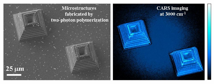
Two-photon polymerization (TPP) is an enabling technology that allows fast prototyping of parts with feature sizes smaller than 100 nm. Due to its ability to fabricate microstructures with arbitrary three-dimensional geometries, TPP has been employed in diverse fields such as photonics, microelectronics, microelectromechanical systems, microfluidics, and bioengineering. However, no information is available to date that microscopically correlates the experimental conditions used in TPP with the properties of the ultimate microstructure. A study is presented where the distribution of polymer cross-linking in three-dimensional microstructures fabricated by TPP is visualized by means of nonlinear microscopy. In particular, coherent anti-Stokes Raman scattering (CARS) microscopy is employed to image polymer microstructures with chemical specificity. The characterization of the microstructures based on the acquired images permits rational optimization of the TPP process.
Two-photon polymerization (TPP) is an enabling technology that allows fast prototyping of parts with feature sizes smaller than 100 nm. Due to its ability to fabricate microstructures with arbitrary three-dimensional geometries, TPP has been employed in diverse fields such as photonics, microelectronics, microelectromechanical systems, microfluidics, and bioengineering. However, no information is available to date that microscopically correlates the experimental conditions used in TPP with the properties of the ultimate microstructure. A study is presented where the distribution of polymer cross-linking in three-dimensional microstructures fabricated by TPP is visualized by means of nonlinear microscopy. In particular, coherent anti-Stokes Raman scattering (CARS) microscopy is employed to image polymer microstructures with chemical specificity. The characterization of the microstructures based on the acquired images permits rational optimization of the TPP process.
Bio:
After studying Chemistry at the University of Rome “La Sapienza”, Tommaso Baldacchini pursued doctoral research at Boston College. Under the guidance of Professor John T. Fourkas, he worked on unconventional methods to fabricate three-dimensional microstructures and received a Ph.D. in Physical Chemistry in 2004. He then joined the research group of Professor Eric Mazur at Harvard University as a postdoctoral fellow, where his work focused on the wettability properties of micro- and nano-structured surfaces prepared by femtosecond laser ablation. In 2006 he joined the Technology and Applications Center at Newport Corporation as a Staff Scientist. His research interests lie in the applications of nonlinear optics in microscopy and nanofabrication.
After studying Chemistry at the University of Rome “La Sapienza”, Tommaso Baldacchini pursued doctoral research at Boston College. Under the guidance of Professor John T. Fourkas, he worked on unconventional methods to fabricate three-dimensional microstructures and received a Ph.D. in Physical Chemistry in 2004. He then joined the research group of Professor Eric Mazur at Harvard University as a postdoctoral fellow, where his work focused on the wettability properties of micro- and nano-structured surfaces prepared by femtosecond laser ablation. In 2006 he joined the Technology and Applications Center at Newport Corporation as a Staff Scientist. His research interests lie in the applications of nonlinear optics in microscopy and nanofabrication.

|
|
